Electronic Devices and Design Laboratory
Edition: 1
Copyright: 2017
Pages: 298
Choose Your Format
$68.07 USD
The recent invention of the Texas Instruments Education Transistor Array IC, EDU1000, makes modern CMOS experiments accessible to undergraduates. The Electronic Devices and Design Laboratory is designed to provide the background and tools for students to simulate and design, build and test circuits that cover fundamental devices of modern electronics. The Deliverables section establishes standards for application of tools from Thevenin equivalent circuits to load lines and for reporting work. A consistent respect for the correct employment of Linear Time Invariant Analysis is maintained.
The book is focused on the fundamentals and applications of signal diodes, bipolar transistors, and MOSFET transistors. Students design test sets to investigate the fundamentals of these devices. Then, they apply large and small signal analysis techniques with design, build, and test applications:
1. Signal Diode:
a. Triangle-to-Sine Waveform Converter
b. Voltage-Controlled Attenuator
2. Bipolar Transistor:
a.Precision Gain Amplifier
b. Student Made Transistor Curve Tracer
3. MOSFET:
a. CMOS Inverter
b. Motor Drive—Power MOSFET
c. Common Source with Current Mirror
d. Differential Amplifier with Current Mirror and Active Load
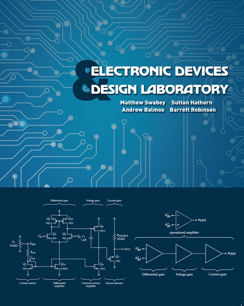
e. Operational Amplifier with Current Mirror and Active Load
Acknowledgments
Online Resources
Contents
I Deliverables
I.1 The engineering method
I.2 Signal naming convention
I.3 Measure
I.4 Plot
I.5 Circuit diagram
I.6 Design a circuit
I.7 Thévenin equivalent circuit
I.8 I–V characteristic plots of two-terminal devices
I.8.1 Looping in I–V curves
I.9 Load lines
I.10 Measuring time-domain gain
I.11 Simulations
I.12 References
1 Introduction Experiment
1.1 Instructional objectives
1.2 Application
1.3 What is common? What is ground?
1.3.1 Example: A building electrical service
1.4 Two-terminal devices
1.5 Two-port devices
1.6 Lab equipment
1.6.1 Oscilloscopes
1.6.2 Differential amplifiers
1.6.3 Function generators
1.7 Tasks
1.8 References
2 Measurement of Diode Characteristics
2.1 Instructional objectives
2.2 Application
2.3 Prelab
2.4 The ideal pn diode equation
2.5 The 1N4148 fast switching diode
2.6 A quick method for testing diodes
2.7 References
3 Triangle to Sine Converter Design
3.1 Instructional objectives
3.2 Application
3.3 Prelab
3.4 Piecewise linear models for diodes
3.4.1 The ideal diode
3.4.2 The ideal diode with a battery
3.4.3 The ideal diode with a battery and resistor
3.4.4 Selecting a model and its parameters:
3.4.5 Test set to measure Vo and Ro
3.5 Voltage transfer characteristics
3.5.1 Measuring a voltage transfer characteristic
3.6 Triangle to sine wave converter
3.6.1 Circuit design
3.7 Tasks
4 A Small Signal Attenuator
4.1 Instructional objectives
4.2 Application
4.3 Prelab
4.4 Small signal analysis
4.5 The voltage divider as an attenuator
4.6 The semiconductor diode as a variable resistor
4.6.1 A variable voltage attenuator
4.6.2 Derivation of diode small signal resistance rd from the ideal diode equation
4.6.3 Determination of ηVT and Io from I–V data
4.6.4 DC blocking capacitors
4.7 Tasks
4.8 Semi-log graph paper
4.9 References
5 Large Signal Model for Bipolar Transistors
5.1 Instructional objectives
5.2 Application
5.3 Prelab
5.4 BJT structure
5.4.1 Type and base identification
5.4.2 Emitter and collector identification
5.5 BJT large signal operation
5.5.1 Cutoff
5.5.2 Saturation
5.5.3 Active
5.5.4 Reverse active
5.6 BJT test sets
5.6.1 Collector I–V test set
5.6.2 Base I–V test set
5.7 BJT parameters
5.7.1 Estimating collector-emitter leakage current (ICE0)
5.7.2 Estimating large signal current gain (β)
5.7.3 Estimating RBB and Vo
5.7.4 Complete large signal model
5.8 Tasks
5.9 References
6 Lab Practical 1
6.1 Paper-and-pencil problems
6.2 Circuit construction problem
6.3 Simulation problem
6.4 Follow-up questions
7 A Student Made Curve Tracer
7.1 Instructional objectives
7.2 Application
7.3 Prelab
7.4 Overview
7.5 Large signal current gain (β) and small signal current gain (β0)
7.6 Operation of the curve tracer
7.7 Tasks
7.8 Formal report
7.9 References
8 Common Emitter: Biasing and Small Signal Properties
8.1 Instructional objectives
8.2 Application
8.3 Prelab
8.4 Background
8.4.1 Linear and time invariant (LTI) systems
8.5 Common emitter amplifier
8.5.1 Input and output impedance
8.5.2 There is more than one right answer
8.6 Tasks
8.7 Load line plot of an undistorted output
8.8 Load line plot of an output distorted by saturation
8.9 Load line plot of an output distorted by cut-off
9 Common Emitter: Precision Gain Amplifier
9.1 Instructional objectives
9.2 Application
9.3 Prelab
9.4 Hybrid-π model
9.4.1 Transconductance, gm
9.4.2 Base emitter resistance, rπ
9.4.3 Output resistance, ro
9.5 Common emitter amplifier with emitter degeneration
9.5.1 Small signal circuit
9.5.2 DC biasing
9.5.3 DC blocking capacitor selection
9.6 Precision gain common emitter amplifier
9.6.1 System input resistance
9.6.2 System output resistance
9.6.3 System gain
9.7 Tasks
10 CMOS Inverter
10.1 Instructional objectives
10.2 Application
10.3 Prelab
10.4 CMOS inverter
10.5 Voltage transfer characteristic
10.6 Noise margins
10.7 The CD4007UB dual complementary pair plus inverter
10.8 An oscillator circuit application for the CD4007UB
10.8.1 Operation
10.9 A test set to obtain typical transfer characteristics
10.10 Tasks
10.11 References
11 Motor Drive — Power MOSFET
11.1 Instructional objectives
11.2 Application
11.3 Prelab
11.4 Metal-oxide-semiconductor field-effect transistor (MOSFET)
11.5 Characteristic curves
11.6 MOSFET RDS
11.7 Power control by pulse width
11.8 A test set to obtain typical output characteristics for an IRL530N (low current)
11.9 Tasks
11.10 References
12 Common Source Amplifier
12.1 Instructional objectives
12.2 Application
12.3 Prelab
12.4 MOSFET small signal model
12.4.1 Calculating gm for a MOSFET
12.4.2 Channel length modulation
12.5 Resistor biased common source amplifier
12.6 Current mirrors
12.6.1 Mirror analysis
12.7 Current mirror biased common source amplifier
12.7.1 Picking RD and IBIAS
12.7.2 Picking R1 and R2
12.7.3 Picking C1 and C2
12.8 Tasks
13 MOSFET Differential Amplifier with Current Mirror
13.1 Instructional objectives
13.2 Application
13.3 Prelab
13.4 Background
13.5 The differential amplifier
13.5.1 Differential versus common mode input
13.5.2 The non-ideal differential amplifier
13.5.3 Measuring the performance of a differential amplifier: Common mode rejection ratio
13.6 Differential amplifier
13.6.1 Large signal analysis
13.6.2 The active load
13.7 Ratioed current mirror
13.8 Mirror analysis
13.9 Complete differential amplifier circuit
13.10 Tasks
13.11 References
14 MOSFET Operational Amplifier
14.1 Instructional objectives
14.2 Application
14.3 Prelab
14.4 Design of an operational amplifier
14.5 Extending a differential amplifier to an operational amplifier
14.5.1 More gain: Common source amplifier
14.5.2 Lowering the output impedance: Source follower
14.6 Tasks
14.7 References
15 Lab Practical 2 — CMOS Operational Amplifier
15.1 Paper and pencil problems
15.2 Circuit construction problems (190)
A IEEE 315-1975 Designators
A.1 References
B Preferred Number Series for Parts Selection
B.1 References
C Datasheets
#53 lamp
1N4148
2N3904
PN2222A
PN2907A
IRL530N
CD4007UB
74HC193
LF356N
EDU1000